
TM 11-5820-921-40-1
2-136. When the +19Vdc is applied to the-14Vdc power supply circuit, square wave generator lAlUl
generates a 20 kHz square wave (pin 4 of 1A1U1 ) which is voltage amplified by transistor 1AlQ1 and
current amplified by transistors 1A1Q2 and Q3. This amplified square wave is coupled through capacitor
1A1C4 to rectifiers 1A1CR2 and CR3. During the positive half cycle, diode 1A1CR3 provides a short circuit
to ground. During the negative half cycle, capacitor 1A1C5 is charged through diode 1A1CR2 to approxi-
mately -14 Vdc. Transistor lA1Q1 and diode 1AlCR1 provide a discharge path for coupling capacitor
1A1C4.
2-138. The +1600 Vdc High Voltage Power Supply consists of three main functional circuit groups:
a.
The De-to-De Converter lA14A3 (see figures 2-11, 3-78 and 3-77) is a power oscillator which
consists of transistors 1A14A3Q1 and Q2, two ferrite beads labeled 1A14A3T 1, and base feedback
transformer 1Al3T1 (part of HV Module Assembly 1A13). When the HV ON signal (ground) from
DC Control PWB Assembly 1A2 energizes the HV START relay 1A13A1K1, transistors 1A14A3Q1
and Q2 oscillate at approximately 2 kHz. Transformers 1A14T1 and 1 A13A1T1 are phased to
sustain oscillation, and resistors 1A14A3R1 and R2 are used to limit the base current of transistors
1A14A3Q1 and Q2.
The high voltage circuit consists of the secondary winding of step-up transformer 1A14T1, diode
b.
bridges 1A13CR1 and CR2, filter capacitor 1A13C1, and bleeder resistors 1A13A1R1 through
R7. The stepped-up voltage from 1A14T1 is rectified by diode bridges 1A13CR 1 and CR2 and
filtered by capacitor 1A13C1. Bleeder resistors 1Al3A1R1 through R7 across the high voltage
output provide a quick discharge of the 2.0 u F1Al3C1 capacitor when the PA is switched off and
also derive the 1600V SENSE signal that is sent to the metering circuit and used to actuate indica-
tor light 1A13A1DS1.
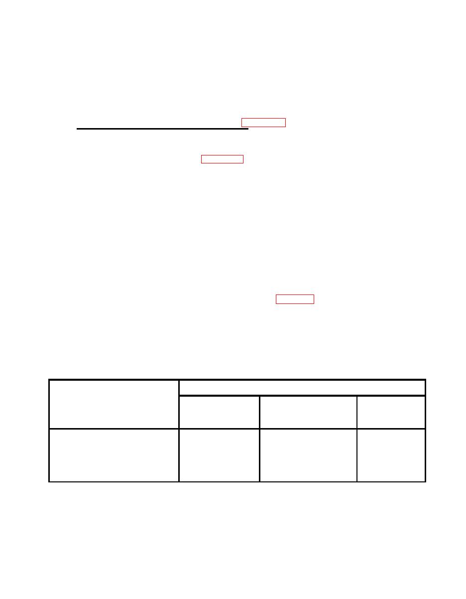
Control Circuit - The active elements of the dc-to-dc converter control circuits operate in the
c.
two-state switching mode. They are either ON or OFF. Table 2-6 shows the operating states of the
active elements under three operating conditions:
(1) When primary power is switched ON.
(2) During normal operation after the 60 second warm-up time delay and with the transmitter
keyed.
(3) During a FAULT.
OPERATING CONDITION
A
c
B
PRIMARY POWER
PA FAULT
SWITCHED ON
NORMAL OPERATION
ACTIVE CONTROL ELEMENT
0
1
0
1A13A1K1
1
0
0
1A2Q7
0
0
1
1A2Q8
0
0
1*
1A13A1Q1
0
1
1
1A2U1-3
LEGEND: 1 = ON (Transistor saturated or relay energized)
0 = OFF (Transistor cutoff or relay de-energized)
* = Pulse output to start power oscillator transistor 1A13A1Q1, then open.
2-33/(2-34 blank)

