
TM 11-5820-921-40-1
1A8A4B1, causing it to rotate and turn switch wafers S1-A, S1-B, and S 1-C through a set of speed reduction
gears. The motor (1A8A4B1) will continue to move the switch rotors until the 1A8A4S1 -A wiper touches
the contact 2 switch position that now has the grounded BAND CODE signal applied to it. The instant this
occurs, the SWITCH WIPER signal to the band control circuit is grounded, turning transistors 1A6Q11 ON,
1A6Q9 OFF, 1A6Q12 ON, and 1A6Q10 OFF. This disconnects the +19 Vdc from the BAND MOTOR +
signal line through 1A6Q10 and grounds the BAND MOTOR (+) signal line and the MOTOR (-) GND
signal line together through transistor 1A6Q12 for dynamic breaking, causing the motor to stop with all
switch rotor contacts in position 2. This position selects capacitor 1A8A1C12 for the input to the pi -
network and capacitors 1A8A2AC24 and C25 for the output of the pi-network, tuning the pi-network to
the F frequency band (12 -16 MHz),
2-83. The power amplifier receives six lines of binary coded decimal frequency input information
RT-1209/URC via Amplifier-Converter AM-6879/GRC-l 93. These signals are applied to Band Control PWB
Assembly 1A6 thru RT CONTROL connector 1A14J2 and Interconnection PWB Assembly 1A14A1. Band
code generation is the process of converting the six BCD (Binary Coded Decimal) input frequency codes
into nine discrete BAND CODE signal lines (X, A, B, C, D, E, F, G, and H). BAND CODE X is an invalid
band code which is used to generate the BANDSWITCH INHIBIT signal described in paragraph 2-84. The
remaining BAND CODE signal lines (A thru H) are used to position the bandswitch drive motor 1A3A4B1
through the band motor control circuitry described in paragraph 2-77. Table 2-1 shows the direct relation-
ship of the BCD input signal frequency codes, the BAND CODE signals, and their corresponding 28 usable
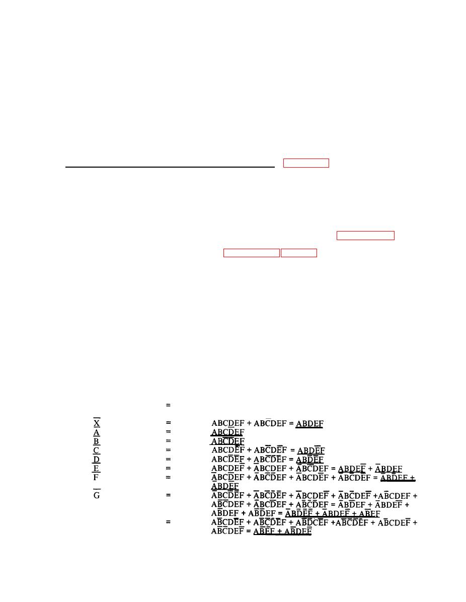
frequency ranges. Using the letter designations A through F for the six binary inputs, with a dash above
the letter to indicate the binary " 1" state (high), the simplifications shown in table 2-12 can be written.
significant and need be considered. The actual code conversion process is performed in three columns of
gates, 1A6U1 through 1A6U9, by combining pairs of digits in each term of the expression. For example,
when the selected frequency is 2.6750 MHz, the code conversion expression A = ABCDEF must be satisfied
to get a logic " 1" (high) signal at the BAND A output terminal. In the first column of AND gates, the in-
verted A output, at 1A6U1-3, is combined with the inverted B output at 1A6U1-4, to produce the logic
"1" (high) AB output, at 1A6U6-3. The inverted E output, at 1A6U24, is combined with the inverted F
output, at 1A6U1-11, to produce the logic " 1" (high) EF output at 1A6U3-11. The inverted C output, at
1A6U1-10, is combined with the direct D code line, from 1A6P1-2, to produce the logic " 1" (high CD
output, at 1A6U5-3.
BAND CODE
BCD BIT DESIGNATION
H

